Saturday, 30 November 2013

Week 1 of FYP 2

Date : 03/02/2014 (Monday)
Title  : Research and findings (LM 1117T – Voltage Regulator)


ANALYSIS


Pin Configuration of LM 1117T

Friday, 29 November 2013

Week 2 of FYP 2

Date : 10/02/2014 (Monday)
Title  : Find the right component and tools for the project

- Buy the component from electronics shop in Jalan Pasar by referring to each of schematics circuit.
- Buy some tools that are used to make the project like soldering iron, drill, copper board and sand paper.


List of components needed for Relay Circuit
  • ·         Relay 12 Volt
  • ·         Transistor NPN 2222
  • ·         Resistor 1kΩ (x2 unit)
  • ·         Diode


List of components needed for PIC circuit
  • ·         40-Pin IC socket
  • ·         PIC 16F877A
  • ·         Resistor 1kΩ (x2 unit)
  • ·         Oscillator 20 MHz (crystal)
  • ·         Capacitor 18pf (x2 unit)
  • ·         LED
  • ·         Capacitor 0.1µf (x2 unit)
  • ·         LM 7805 (voltage regulator)


List of components needed for Bluetooth circuit
  • ·         Bluetooth Module (HC-05)
  • ·         LM1117T (voltage regulator)
  • ·         Capacitor 100nf (x2 unit)


Other components and tools

  • ·         Pin header
  • ·         Pin header connector
  • ·         Adapter 12V (x2 unit)
  • ·         Solenoid 12V
  • ·         Jumper wire
  • ·         LCD Display


Thursday, 28 November 2013

Week 3 of FYP 2

Date : 20/02/2014 (Thursday)

Title  : Testing circuits and design the PCB Layout

- Testing each circuit on breadboard to make sure the circuit is functioning well.

- After each circuit has been tested, Dip-Trace Software is used in this project for designing the PCB Layout

PCB Layout Design For PIC Circuit

PCB Design of PIC Circuit


PCB Layout Design For Relay Circuit


PCB Design of Relay Circuit

Wednesday, 27 November 2013

Week 4 of FYP 2

Date : 28/02/2014 (Friday)
Title  : FYP Briefing

Briefing conducted at 3 pm

- The briefing is about to give some explanation for the students who are taking the final project for Diploma and Degree programmes. The briefing is about:


·         Introduction
·         Objectives
·         Credits and duration
·         Scope of projects
·         Title selection
·         Project Assessment
·         Presentation day
·         Submission date of project

Tuesday, 26 November 2013

Week 5 of FYP 2

Date : 05/03/2014 (Wednesday)

Title  : Etching process on the copper board according to the PCB layout 


This is the result of PCB Layout design using Dip-Trace software. Design is ready to be printed using Toner Printer (carbon ink). The next step is to attach PCB layout on the copper board.

 
Clothes iron will be used to iron the PCB design to attach on the surface of copper board.


After attaching the PCB design on to the copper board. It will be placed into the etching acid. This process takes about 20 minutes to remove the remaining copper that is not needed.

- The simplest method, used for small-scale production and often by hobbyists, is immersion etching, in which the board is submerged in etching solution such as ferric chloride. Compared with methods used for mass production, the etching time is long. Heat and agitation can be applied to the bath to speed the etching rate. In bubble etching, air is passed through the etchant bath to agitate the solution and speed up etching

- Chemical etching is usually done with ammonium persulfate or ferric chloride. For my project, Ferric Chloride Anhydrous powder is used for etching process.


- The results of the etching process. Copper is not needed will be eroded, only copper that covered by carbon ink will remain on the board and form a circuit.

Monday, 25 November 2013

Week 6 of FYP 2

Date : 11/03/2014 (Tuesday)
Title  : Make a drilling process after etching the circuit design

-Holes through a PCB are typically drilled with small-diameter drill bits made of solid coated  tungsten carbide. Coated tungsten carbide is recommended since many board materials are  very abrasive and drilling must be high RPM and high feed to be cost effective. Drill bits must  also remain sharp so as not to mar or tear the traces. Drilling with high-speed-steel is simply  not feasible since the drill bits will dull quickly and thus tear the copper and ruin the boards.


-In this project, I am using the Pro’s Kit super mini drill 12V to make the drilling process.


Next, drill the holes using a driller.


This is the result after the board had been rubbed by sandpaper to remove the remaining copper that not been covered by carbon ink. Lastly, this circuit is ready to be constructed with the components.

Sunday, 24 November 2013

Week 7 of FYP 2

Date : 20/03/2014 (Thursday)
Title  : Apply the components on copper board and do the soldering process

- To solder the components on the board according to the PCB design for each circuit.

- To make a connection for all component on the copper board.


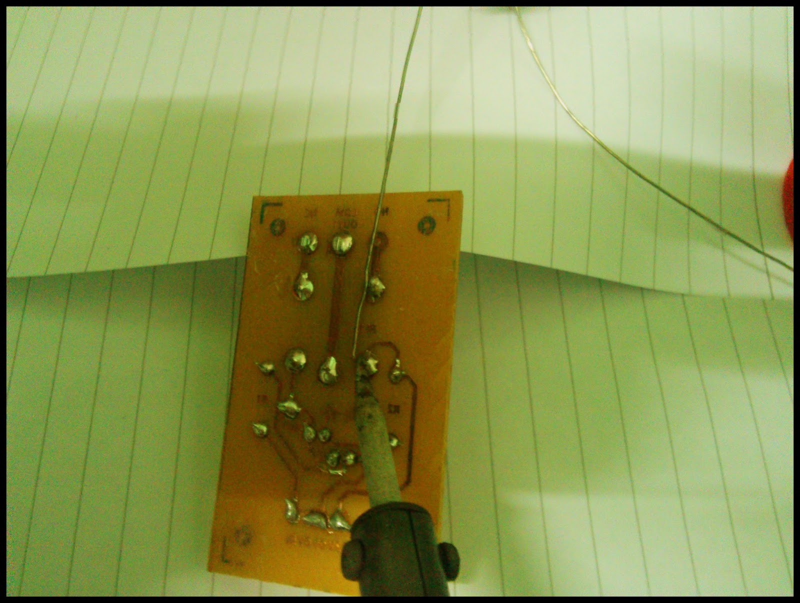
Soldering Components on PIC Circuit


Soldering Components on Relay Circuit


Top View of PIC Circuit


Top Bottom of PIC Circuit


Top View of Relay Circuit


Bottom View of Relay Circuit

Troubleshooting The Circuit

- After soldering the entire component on the copper board. The circuit must undergo troubleshooting to check whether the components are properly connected according to the PCB layout.

Saturday, 23 November 2013

Week 8 of FYP 2

Date : 03/04/2014 (Thursday)

Title  : Bluetooth Module circuit 


ANALYSIS

-Bluetooth Module is no need to be soldered on its pin as compare to the other circuits that  have been done in previous week since it is just “Plug & Play”.

-The Bluetooth module works on 3.3V level only. High voltage like 5V will permanently damage the module. Therefore, if application requires to be operated at 5V then use a LM1117-3.3 regulator to convert the 5V level to 3.3V level as required by module. By considering this factor, I have to add the LM1117T circuit since the supply voltage from the PIC is 5V. From here, LM 1117T will do its task by reducing the voltage from 5V to 3.3V as required by HC-05 Bluetooth Module


Full View of Bluetooth Module Circuit


Friday, 22 November 2013

Week 9 of FYP 2

Date : 08/04/2014 (Tuesday)
Title : MQ-4 Semiconductor Sensor for Natural Gas


Description:

          Sensitive material of MQ-4 gas sensor is SnO2, which with lower conductivity in clean air. When the target combustible gas exist, the sensor’s conductivity is higher along with the gas concentration rising. Please use simple electro circuit, Convert change of conductivity to correspond output signal of gas concentration.
MQ-4 gas sensor has high sensitivity to Methane, also to Propane and Butane. The sensor could be used to detect different combustible gas, especially Methane; it is with low cost and suitable for different application.


Character: 

  • ·         Good sensitivity to Combustible gas in wide range.
  • ·         High sensitivity to LPG, Propane and Hydrogen.
  • ·         Long Life and Low Cost.
  • ·         Simple drive circuit.


Application:

  • ·         Domestic gas leakage detector.
  • ·         Industrial Combustible gas sensor.
  • ·         Portable gas sensor.


Configuration:

Sensor Pin Configuration


Technical Data:

Sensor Technical Data


Basic Test Loop:

Sensors Basic Test Loop

The above is basic test circuit of the sensor. The sensor needs to be put two voltage, heater voltage (VH) and test voltage (VC). VH used to supply certified working temperature to the sensor, while VC used to detect voltage (VRL) on load resistance (RL) whom is in series with sensor. The sensor has light polarity, Vc need DC power. VC and VH could use same power circuit with precondition to assure performance of sensor. In order to make the sensor with better performance, suitable RL value is needed:


Power of Sensitivity body (Ps):


Resistance of sensor (Rs):


Sensitivity Characteristics:

Sensors Sensitivity Characteristics

Fig.1 shows the typical sensitivity characteristics of the MQ-4, ordinate means resistance ratio of the sensor (Rs/Ro ), abscissa is concentration of gases. Rs mean resistance in different gases, Ro means resistance of sensor in 1000ppm Methane. All tests are under standard test conditions.

P.S.: Sensitivity to smoke is igniting 10pcs cigarettes in 8m3  rooms, and the output equals to 200ppm Methane.


Influence of Temperature/Humidity:

Sensors Temperature/Humidity Influences

Fig.2 shows the typical temperature and humidity characteristics. Ordinate means resistance ratio of the sensor (Rs/Ro ), Rs means resistance of sensor in 1000ppm Methane under different temperature and humidity., Ro means resistance of the sensor in environment of 1000ppm Methane, 20˚C/65%RH

Structure and Configuration: 

Sensors Structure and Configuration

Structure and configuration of MQ-4 gas sensor is shown as Fig. 3, sensor composed by micro AL2O3 ceramic tube, Tin Dioxide (SnO2) sensitive layer, measuring electrode and heater are fixed into a crust made by plastic and stainless steel net. The heater provides necessary work conditions for work of sensitive components. The enveloped MQ-4 has 6 pin, 4 of them are used to fetch signals, and other 2 are used for providing heating current.